
News Summary
The University of Arizona has expanded its high-tech Nanofabrication Core Facility, enhancing the state’s leadership in the semiconductor industry. This strategic investment aims to create job pathways for students and supports Arizona’s emergence as a national hub for technological innovation. Equipped with state-of-the-art tools, the facility will foster workforce development and partnerships, significantly contributing to Arizona’s economic growth in high-demand technical fields.
Phoenix, AZ — The University of Arizona (U of A) has significantly bolstered the state’s leadership in the rapidly expanding semiconductor industry with the opening of its newly expanded high-tech Nanofabrication Core Facility. This strategic investment in cutting-edge research infrastructure is poised to create robust job pathways for students, further solidifying Arizona’s position as a national hub for advanced manufacturing and technological innovation. The facility, part of the U of A’s Center for Semiconductor Manufacturing, represents a commitment to academic rigor and practical, hands-on learning, designed to cultivate a highly skilled workforce essential for the state’s economic future.
The expansion underscores a collaborative vision, uniting academic excellence with state economic development initiatives. By providing students with access to state-of-the-art tools and real-world manufacturing environments, the U of A is ensuring that graduates are not only academically proficient but also immediately workforce-ready. This approach aligns with broader statewide efforts to bridge the talent gap in high-demand technical fields, fostering personal responsibility and discipline among students while contributing meaningfully to the community’s economic vitality.
Catalyzing Arizona’s Semiconductor Renaissance
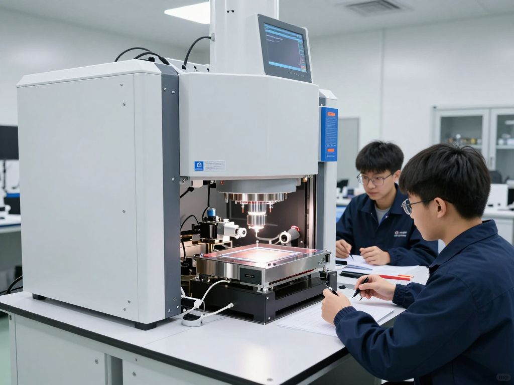
The newly expanded Nanofabrication Core Facility, located within the Electrical and Computer Engineering Building in Tucson, represents a critical asset for Arizona’s burgeoning semiconductor sector. This specialized clean room, which now spans 6,800 square feet, significantly increases the university’s capacity for advanced research and development in microelectronics. The facility is equipped with ultramodern tools necessary for critical steps in producing nanoscale technology, including wafer polishing, photolithography, etching, metrology, and packaging. The meticulously controlled environment maintains an air purity level 10,000 times cleaner than outside air, a testament to the precision required for semiconductor fabrication.
This expansion was made possible by a substantial $35.5 million award from the Arizona Commerce Authority (ACA) in 2023. This funding not only facilitated the physical enlargement and equipping of the facility but also earmarked $4.5 million specifically for statewide workforce development programs. This investment highlights a proactive strategy to cultivate a talent pipeline capable of sustaining Arizona’s rapid growth in the semiconductor industry, which has seen over $210 billion in related investments and more than 25,000 projected new jobs across the state since 2020.
Building the Future Workforce: Hands-On Pathways
A cornerstone of the U of A’s initiative is the creation of diverse and accessible educational pathways tailored to the demands of the semiconductor industry. The university now offers a comprehensive suite of programs designed to prepare students for high-tech careers. These include an undergraduate minor degree in semiconductor manufacturing, stackable graduate degree certificates covering semiconductor materials, processing, and packaging, and an accelerated master’s program in semiconductors. Furthermore, a co-curricular ‘Fast-track’ digital certificate program is available for both STEM and non-STEM majors, ensuring broad access to specialized training.
The learning experience within the new lab is highly immersive, emphasizing hands-on training and the use of advanced simulation tools. Students gain practical experience operating industry-standard equipment, translating theoretical knowledge into applied skills. Notably, undergraduates are utilizing technologies such as Apple Vision Pro and Meta Quest 3 headsets to explore digital twins of the cleanroom and its equipment, providing an innovative and safe environment for learning complex procedures. This integration of virtual and physical learning environments reflects a forward-thinking approach to technical education, preparing students for the advanced technological landscapes they will encounter in their careers.
Strategic Collaborations and Statewide Impact
The impact of the U of A’s expanded facility extends beyond the campus, fostering strategic collaborations that strengthen Arizona’s entire educational and economic ecosystem. The university is a key partner in the Southwest Nano-Lab Alliance, a coalition that includes Arizona State University, Northern Arizona University, the University of Utah, the University of New Mexico, and Rio Salado College. This alliance facilitates collaborative workforce initiatives, pooling resources and expertise to address regional and national semiconductor workforce needs.
Additionally, the U of A has formalized an agreement with the National Yang Ming Chiao Tung University (NYCU) in Taiwan, aiming to redefine workforce development in a globally interconnected high-tech economy. This international partnership underscores Arizona’s ambition to be a global leader in semiconductor manufacturing and research. Beyond higher education, the U of A also engages in K-12 outreach programs, such as the Chips and Wafers Camp developed with the Chandler Unified School District. These programs introduce high school students to the industry early, building a foundational pipeline of future talent.
Driving Arizona’s Economic Fortunes
The expansion of the Nanofabrication Core Facility is a vital component of Arizona’s broader economic development strategy, particularly in positioning the state as a dominant force in the semiconductor industry. Arizona has emerged as a national leader in new semiconductor ecosystem investment, attracting over $102 billion since the inception of the CHIPS Act. This surge in investment has led to more than 40 new projects and generated over 15,700 industry jobs, with a statewide projection of over 25,000 new jobs since 2020.
University of Arizona President Suresh Garimella highlighted that Arizona’s emergence as a national hub for semiconductor manufacturing relies on innovation, technical expertise, and a highly skilled workforce. Governor Katie Hobbs emphasized that Arizona has stepped forward to increase domestic manufacturing capacity, crucial for modern life and national security. Sandra Watson, President and CEO of the Arizona Commerce Authority, noted that the facility reinforces Arizona’s standing as an epicenter for pioneering semiconductor innovation and investment. This collective effort ensures that educational advancements directly translate into economic growth and job creation across the state, including the vibrant employment markets in the greater Phoenix area.
Summary of Key Features and Economic Impact
| Feature/Metric | Details |
|---|---|
| Facility Name | Nanofabrication Core Facility, Center for Semiconductor Manufacturing |
| Location | Electrical and Computer Engineering Building, University of Arizona, Tucson |
| Clean Room Size Expansion | From 2,800 to 6,800 square feet |
| ACA Funding (2023) | $35.5 million total, with $4.5 million for workforce development |
| Statewide Semiconductor Investments (since 2020) | Over $210 billion |
| Projected New Semiconductor Jobs (since 2020) | Over 25,000 |
| Key Programs | Undergraduate minor, graduate certificates, accelerated master’s, digital certificate, K-12 outreach |
| Technological Integration | Apple Vision Pro, Meta Quest 3 for digital twins |
A Commitment to Leadership and Innovation
The University of Arizona’s expanded Nanofabrication Core Facility is more than an advanced laboratory; it is a testament to the power of disciplined investment in education and research to shape a state’s future. By equipping students with the knowledge and practical skills required for the semiconductor industry, the U of A is actively contributing to the development of future leaders and innovators. This initiative reflects a core belief in academic freedom, personal responsibility, and the profound impact that institutions of higher learning can have on local and national prosperity. The collaborative spirit and commitment to excellence embedded in this project will undoubtedly continue to drive Arizona’s technological leadership and provide unparalleled opportunities for its citizens.
Readers interested in the evolving landscape of Arizona higher education and its contributions to the state’s economic and technological advancements are encouraged to explore the various programs offered by the University of Arizona and other institutions across the state. Staying informed about Phoenix AZ college news and university developments, especially in critical sectors like the semiconductor industry Arizona, offers insights into the pathways shaping our collective future.
Frequently Asked Questions
What is the Nanofabrication Core Facility?
The Nanofabrication Core Facility is an expanded high-tech lab at the University of Arizona, part of its Center for Semiconductor Manufacturing. It is a clean room equipped with ultramodern tools for critical steps in producing nanoscale technology.
Where is the Nanofabrication Core Facility located?
It is located within the Electrical and Computer Engineering Building at the University of Arizona in Tucson.
What is the primary purpose of the expanded lab?
The primary purpose is to advance research, innovation, and workforce development in the semiconductor sector, creating job pathways for students and strengthening Arizona’s semiconductor industry.
How was the expansion of the lab funded?
The expansion received $35.5 million in funding from the Arizona Commerce Authority (ACA) in 2023, with $4.5 million specifically allocated for statewide workforce development.
What types of programs are offered to students at the facility?
The facility supports an undergraduate minor degree in semiconductor manufacturing, stackable graduate degree certificates in semiconductor materials, processing, and packaging, an accelerated master’s program in semiconductors, and a co-curricular ‘Fast-track’ digital certificate program for both STEM and non-STEM majors.
How does the lab prepare students for jobs in the semiconductor industry?
It prepares students through hands-on training, advanced simulation tools, and partnerships, including the use of Apple Vision Pro and Meta Quest 3 headsets for digital twins of the cleanroom and equipment.
What is the clean room’s air purity level?
The clean room’s air is 10,000 times cleaner than outside air, essential for the precision required in chip manufacturing.
What is the statewide impact of this initiative on Arizona’s economy?
The initiative contributes to Arizona’s leadership in semiconductor investment, which has seen over $210 billion in related investments and more than 25,000 projected new jobs across the state since 2020.
Deeper Dive: News & Info About This Topic
HERE Resources
University of Arizona Expands Housing and Student Services
Metro Phoenix Tech Sector Drives Arizona’s Economic Growth and Job Creation
Phoenix’s Chip Future: Taiwan Giant Fuels Workforce Innovation
TSMC’s Expansion in Arizona Enhances Tech Education at UA
Tempe Unveils Spring Opportunities for Community Engagement
Arizona’s Economic Ascent: Top 20 Industries to Watch in 2026
Arizona Tech Week Brings Innovation to the Forefront
Phoenix’s Economic Powerhouses: Leaders to Watch in 2026
University of Arizona Expands Semiconductor Research Facility
Arizona’s Economic Engines: 10 Firms Propelling Growth