
News Summary
Applied Materials Inc. and Arizona State University have inaugurated a $270 million semiconductor research facility in Tempe, Arizona. The Materials-to-Fab Center, featuring extensive cleanroom and lab space, aims to advance semiconductor technology and bolster Arizona’s position in the industry. Through collaboration between ASU and Applied Materials, the center is set to produce significant research outcomes and innovations in chip technologies, contributing to both local and national tech leadership.
Tempe, Arizona – Applied Materials Inc. and Arizona State University (ASU) have inaugurated a groundbreaking $270 million semiconductor research, development, and prototyping facility. The new Materials-to-Fab Center aims to bolster Arizona’s evolving semiconductor ecosystem and is strategically located within ASU’s MacroTechnology Works building at the ASU Research Park.
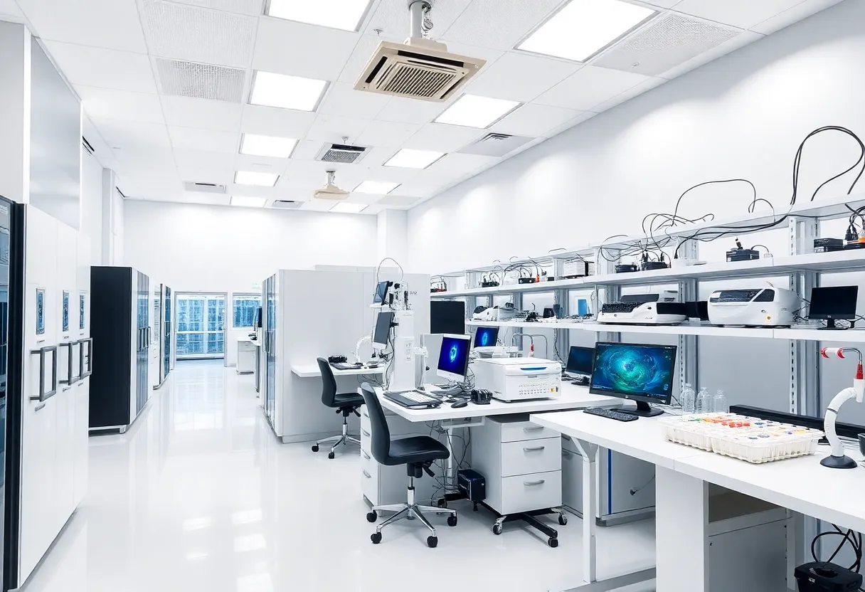
This state-of-the-art center features 50,000 square feet of cleanroom space, complemented by an additional 20,000 square feet dedicated to wet and dry labs. It is designed to facilitate innovation by supporting the transition from initial ideas to the creation of fabrication prototypes. This initiative will play a vital role in advancing new chip technologies that are critical for enhancing U.S. leadership in artificial intelligence (AI) and high-performance computing.
Applied Materials will provide its semiconductor manufacturing equipment within a collaborative environment that engages ASU’s engineering teams, technologists from Applied Materials, and industry partners. This collaboration is expected to yield more than 30 research publications and eight patents, reflecting the center’s commitment to groundbreaking research and innovation since its inception.
Dr. Prabu Raja, president of Applied Materials’ semiconductor products group, highlighted the importance of this facility during the ribbon-cutting ceremony, emphasizing its role in fostering innovation in semiconductor technology.
Features of the Materials-to-Fab Center
The Materials-to-Fab Center is designed to be a hub of research and technological advancement. The extensive cleanroom space is essential for maintaining the required conditions for semiconductor fabrication, while the laboratories will allow for extensive research on developing new materials and processes for chip technologies.
The facility aims to serve as a critical link between academia and industry, where theoretical research and practical applications can come together to create significant advancements in semiconductor technology. By leveraging the resources of both ASU and Applied Materials, the center is poised to make considerable contributions to the field.
Impact on Arizona’s Semiconductor Ecosystem
Arizona has increasingly become a focal point for semiconductor research and manufacturing, attributed to its favorable business climate and investment in technology. The establishment of the Materials-to-Fab Center signifies a continued commitment to enhancing the state’s capabilities in this high-demand sector, particularly as the global demand for semiconductor chips continues to escalate.
The collaboration anticipates yielding important technological developments that support not only local investment in the semiconductor industry but also broader national objectives related to technology leadership and innovation. The expertise and resources pooled by ASU and Applied Materials represent a significant step forward in realizing the potential of Arizona’s semiconductor industry.
Conclusion
As the semiconductor landscape evolves, the Materials-to-Fab Center aims to address the burgeoning demand for advanced chip technologies while supporting workforce development and driving innovation in the field. With its impressive financial backing and collaborative model, the facility stands to contribute meaningfully to both local and national technological advancements for years to come.
Deeper Dive: News & Info About This Topic
HERE Resources
Local Construction Firm in Kannapolis Plans Expansion
Arizona to Host SEMICON West 2025, Boosting Semiconductor Industry
Phoenix Hosts SEMICON West, Highlighting Semiconductor Growth
North Phoenix Development Adds Costco and Hotels
Brewer Science Opens Arizona Innovation Center
Key Leaders Shaping Arizona’s Economic Growth in 2025
Arizona Achieves Major Economic Milestones in FY25
Arizona Launches New Bioscience Roadmap to Boost Economy
TSMC Expands Internship Program in Arizona
TSMC Begins Mass Production in Arizona to Boost U.S. Semiconductor Industry
Additional Resources
- ABC15 News: Chandler Plant to Produce Intel’s Most Advanced US-Made Semiconductor Technology
- Intel Newsroom: Intel Unveils Panther Lake Architecture
- Executive Gov: Amkor’s $7B Expanded Arizona Chips Project
- IEN: Amkor Expands Semiconductor Project in Arizona
- Manufacturing Dive: Amkor’s $7 Billion Semiconductor Project
- Wikipedia: Semiconductor
- Google Search: Semiconductor Technology
- Google Scholar: Semiconductor Research
- Encyclopedia Britannica: Semiconductor
- Google News: Semiconductor Developments